- 您现在的位置:买卖IC网 > Sheet目录250 > SFCF4096H4BK2SA-I-QT-553-SMA (Swissbit NA Inc)FLASH SLC UDMA/MDMA/PIO 4G
�� �
�
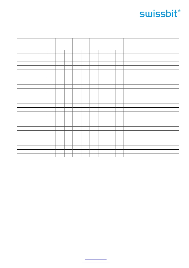
�6.5.4.4� Ultra� DMA� Data� Transfers� Timing�
�Table� 26� and� Table� 27� define� the� timings� associated� with� all� phases� of� Ultra� DMA� bursts.�
�Table 26: Ultra� DMA� Data� Burst� Timing� Requirements�
�Name�
�UDMA�
�Mode� 0�
�(ns)�
�UDMA�
�Mode� 1�
�(ns)�
�UDMA�
�Mode� 2�
�(ns)�
�UDMA�
�Mode� 3�
�(ns)�
�UDMA�
�Mode� 4�
�(ns)�
�Measurement� location�
�(See� Note� 2)�
�Min�
�Max� Min� Max� Min� Max� Min�
�Max� Min� Max�
�t� 2CYCTYP�
�t� CYC�
�t� 2CYC�
�t� DS�
�t� DH�
�t� DVS�
�t� DVH�
�t� CS�
�t� CH�
�t� CVS�
�t� CVH�
�t� ZFS�
�t� DZFS�
�t� FS�
�240�
�112�
�230�
�15.0�
�5.0�
�70.0�
�6.2�
�15.0�
�5.0�
�70.0�
�6.2�
�0�
�70.0�
�230�
�160�
�73�
�153�
�10.0�
�5.0�
�48.0�
�6.2�
�10.0�
�5.0�
�48.0�
�6.2�
�0�
�48.0�
�200�
�120�
�54�
�115�
�7.0�
�5.0�
�31.0�
�6.2�
�7.0�
�5.0�
�31.0�
�6.2�
�0�
�31.0�
�170�
�90�
�39�
�86�
�7.0�
�5.0�
�20.0�
�6.2�
�7.0�
�5.0�
�20.0�
�6.2�
�0�
�20.0�
�130�
�60�
�25�
�57�
�5.0�
�5.0�
�6.7�
�6.2�
�5.0�
�5.0�
�6.7�
�6.2�
�0�
�6.7�
�120�
�Sender�
�Note� 3�
�Sender�
�Recipient�
�Recipient�
�Sender�
�Sender�
�Device�
�Device�
�Host�
�Host�
�Device�
�Sender�
�Device�
�t� LI�
�0�
�150�
�0�
�150�
�0�
�150�
�0�
�100�
�0�
�100�
�Note� 4�
�t� MLI�
�t� UI�
�t� AZ�
�t� ZAH�
�t� ZAD�
�20�
�0�
�20�
�0�
�10�
�20�
�0�
�20�
�0�
�10�
�20�
�0�
�20�
�0�
�10�
�20�
�0�
�20�
�0�
�10�
�20�
�0�
�20�
�0�
�10�
�Host�
�Host�
�Note� 5�
�Host�
�Device�
�t� ENV�
�20�
�70�
�20�
�70�
�20�
�70�
�20�
�55�
�20�
�55�
�Host�
�t� RFS�
�t� RP�
�t� IORDYZ�
�t� ZIORDY�
�t� ACK�
�t� SS�
�160�
�0�
�20�
�50�
�75�
�20�
�125�
�0�
�20�
�50�
�70�
�20�
�100�
�0�
�20�
�50�
�60�
�20�
�100�
�0�
�20�
�50�
�60�
�20�
�100�
�0�
�20�
�50�
�60�
�20�
�Sender�
�Recipient�
�Device�
�Device�
�Host�
�Sender�
�Notes:�
�1.�
�2.�
�3.�
�4.�
�5.�
�6.�
�All� timing� measurement� switching� points� (low� to� high� and� high� to� low)� shall� be� taken� at� 1.5� V.�
�All� signal� transitions� for� a� timing� parameter� shall� be� measured� at� the� connector� specified� in� the�
�measurement� location� column.� For� example,� in� the� case� of� tRFS,� both� STROBE� and� –� DMARDY� transitions�
�are� measured� at� the� sender� connector.�
�The� parameter� tC� YC� shall� be� measured� at� the� recipient’s� connector� farthest� from� the� sender.�
�The� parameter� tLI� shall� be� measured� at� the� connector� of� the� sender� or� recipient� that� is� responding� to� an�
�incoming� transition� from� the� recipient� or� sender� respectively.� Both� the� incoming� signal� and� the� outgoing�
�response� shall� be� measured� at� the� same� connector.�
�The� parameter� tAZ� shall� be� measured� at� the� connector� of� the� sender� or� recipient� that� is� driving� the� bus�
�but� must� release� the� bus� the� allow� for� a� bus� turnaround.�
��Swissbit� AG�
�Industriestrasse� 4�
�Swissbit� reserves� the� right� to� change� products� or� specifications� without� notice.�
�Revision:� 1.51�
�CH-9552� Bronschhofen�
�Switzerland�
�www.swissbit.com�
�industrial@swissbit.com�
�C-300_data_sheet_CF-HxBK_Rev151.doc�
�Page� 31� of� 99�
�发布紧急采购,3分钟左右您将得到回复。
相关PDF资料
SFCF64GBH2BU4TO-I-NU-517-STD
FLASH SLC UDMA/MDMA/PIO 64GB
SFN08B4702CBQLF7
RES ARRAY 47K OHM 7 RES 8-DFN
SFP1050-12BG
FRONT END AC/DC 1050W 12V
SFP450-12BG
PWR SUP 450W 12V 36.6A W/STANDBY
SFSD1024N1BN1TO-I-DF-151-STD
FLASH MICRO SD CARD IND S-200 1G
SFSD2048L1BN2TO-I-DF-151-STD
FLASH SECURE DGTL CARD SD 2G
SFSD4096L1BN2TO-I-Q2-141-STD
FLASH SECURE DGTL CARD SDHC 4G
SFSD8192N1BW1MT-E-QG-111-STD
FLASH MICRO SD 8GB EXT TEMP
相关代理商/技术参数
SFCF64GBH2BU4TO-C-NU-527-STD
制造商:SWISSBIT 功能描述:CFC C-440 DENSITY COMMERCIAL - Trays 制造商:SWISSBIT NA INC 功能描述:FLASH
SFCF64GBH2BU4TO-I-NU-517-STD
功能描述:FLASH SLC UDMA/MDMA/PIO 64GB RoHS:是 类别:存储卡,模块 >> 存储器,PC 卡 系列:C-440 标准包装:30 系列:- 存储容量:8GB 存储器类型:存储卡 - Extreme III SD?
SFCF64GBH2BU4TO-I-NU-527-STD
制造商:SWISSBIT 功能描述:CFC C-440 DENSITY INDUSTRIAL - Trays 制造商:SWISSBIT NA INC 功能描述:FLASH CARD 64GB IND C-440 制造商:Swissbit 功能描述:Memory Cards 64GB IND COMPACT FLASH SLC NAND C440
SFCF8192H1BO2TO-C-Q1-523-SMA
制造商:SWISSBIT NA INC 功能描述:FLASH
SFCF8192H1BO2TO-C-Q1-533-ZP1
制造商:SWISSBIT NA INC 功能描述:FLASH
SFCF8192H1BO2TO-C-Q1-543-SMA
制造商:SWISSBIT NA INC 功能描述:FLASH
SFCF8192H1BO2TOIQ1523SMA
制造商:Swissbit 功能描述:Flash Card 8G-Byte 3.3V/5V CompactFlash 50-Pin
SFCF8192H1BO2TO-I-Q1-523-SMA
功能描述:FLASH SLC UDMA/MDMA/PIO 8G RoHS:是 类别:存储卡,模块 >> 存储器,PC 卡 系列:C-320 标准包装:30 系列:- 存储容量:8GB 存储器类型:存储卡 - Extreme III SD?